
LTCD boot configuration and displaying starting image
Displaying starting image from the bootloader
Section titled “Displaying starting image from the bootloader”Documents used across this example
Section titled “Documents used across this example”- STM32H7S78-DK Schematic: MB1736 Schematic (PDF)
- Reference manual: RM0477 Reference Manual (PDF)
In this example, we will configure the LTDC (LCD-TFT Display Controller) of the STM32H7S78-DK so the bootloader shows a splash image on the screen before jumping to the main application.
The LTDC is a peripheral that continuously reads pixels from a buffer in memory (the frame buffer) and sends them to the display through a parallel RGB interface, together with the synchronization signals (HSYNC, VSYNC, DE and pixel clock). Once it is configured, it works on its own: the CPU does not need to send each pixel, it only tells the LTDC where the image is in memory.
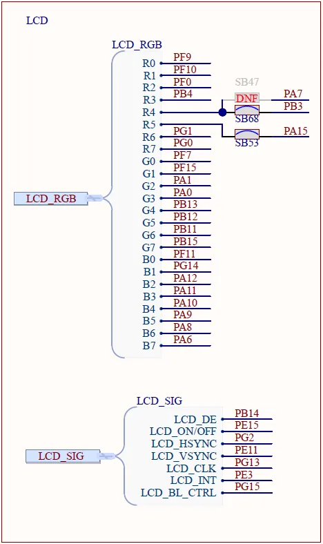
The first step is to know our hardware. In the schematic, you will find the pins that connect the MCU to the screen: the RGB data lines, the synchronization signals, and two extra control signals for turning the display and the backlight on.
MCU initial configuration
Section titled “MCU initial configuration”We are following the previous tutorial Initial Configuration of STM32H7S78-DK with STM32CubeMX: Bootloader Architecture and XIP Application that you can find in learnembeddednow.com. That project already has the boot/application split and the external memory configured in memory-mapped mode, which we will reuse here.
These are the only changes that we are going to make in this example:
CORTEX_M7_BOOT
Section titled “CORTEX_M7_BOOT”The MPU (Memory Protection Unit) defines how the Cortex-M7 can access each memory area: whether it can read, write or execute from it, and whether the cache can be used. In the boot context we have two regions:
- Region 0 is a “background” region that covers the full 4 GB address space with no access permitted. Its purpose is to block speculative accesses from the CPU to addresses where there is no memory, which could otherwise cause unexpected bus errors.
- Region 1 covers the external flash window that starts at
0x70000000(128 MB). It is configured as normal memory (TEX = 1, C = 1, B = 1, which means write-back cacheable) with instruction access enabled. This is the area where the XIP application runs and, in this example, also where our splash image will be stored. Caching only affects the CPU accesses; the LTDC reads the image directly from the bus, and since the image never changes there is no cache coherency issue.
================================================================================CORTEX_M7_BOOT CONFIGURATION - STM32CubeMX================================================================================
[Device and Context]  - Peripheral:                         CORTEX_M7_BOOT  - Runtime contexts:                   Boot (Checked)                                        Application (Unchecked)                                        ExternalMemoryLoader (Unchecked)
[Configuration > Parameter Settings]  > Speculation default mode Settings:    - Speculation default mode:                 Disabled
  > Cortex Interface Settings:    - CPU ICache:                               Enabled    - CPU DCache:                               Enabled
  > Cortex Memory Protection Unit Control Settings:    - MPU Control Mode:                         Background Region Privileged accesses only + MPU Disabled d...
  > Cortex Memory Protection Unit Region 0 Settings:    - MPU Region:                               Enabled    - MPU Region Base Address:                  0x0    - MPU Region Size:                          4GB    - MPU SubRegion Disable:                    0x87    - MPU TEX field level:                      level 0    - MPU Access Permission:                    ALL ACCESS NOT PERMITTED    - MPU Instruction Access:                   DISABLE    - MPU Shareability Permission:              ENABLE    - MPU Cacheable Permission:                 DISABLE    - MPU Bufferable Permission:                DISABLE
  > Cortex Memory Protection Unit Region 1 Settings:    - MPU Region:                               Enabled    - MPU Region Base Address:                  0x70000000    - MPU Region Size:                          128MB    - MPU SubRegion Disable:                    0x0    - MPU TEX field level:                      level 1    - MPU Access Permission:                    ALL ACCESS PERMITTED    - MPU Instruction Access:                   ENABLE    - MPU Shareability Permission:              DISABLE    - MPU Cacheable Permission:                 ENABLE    - MPU Bufferable Permission:                ENABLE================================================================================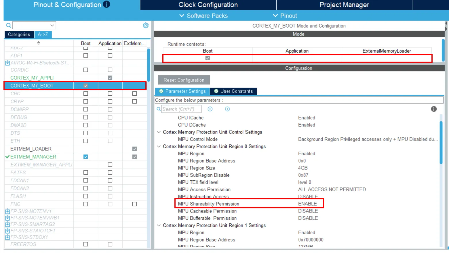
Configuration of the necessary GPIOs to turn on/off the LCD
Section titled “Configuration of the necessary GPIOs to turn on/off the LCD”Besides the RGB and synchronization signals (which are assigned to the LTDC peripheral), the display needs two simple digital signals that we control as normal GPIO outputs:
- PE15 (LCD_ON_OFF): enables the display panel. When it is high, the panel is on.
- PG15 (LCD_BACKLIGHT): enables the backlight. Without it, the panel can be working but you will not see anything because the screen stays dark.
Both are configured as push-pull outputs with an initial level of High, so the display and the backlight turn on as soon as the GPIOs are initialized. The speed is set to Low because these signals only change once (on/off), so there is no need for fast edges, and a lower speed also reduces noise. Since the bootloader is the one showing the image, make sure these pins are initialized in the boot project.
================================================================================GPIO CONFIGURATION - STM32CubeMX (STM32H7S7L8HxH)================================================================================
[Device and Context]  - Microcontroller:             STM32H7S7L8HxH  - Peripheral:                  GPIO  - Runtime Contexts:            Free
[PE15 Configuration]  - Pin Name:                    PE15  - Signal on Pin:               n/a  - Pin Context Assignment:      Free  - GPIO Output Level:           High  - GPIO Mode:                   Output Push Pull  - GPIO Pull-up/Pull-down:      No pull-up and no pull-down  - Maximum Output Speed:        Low  - Peripherals:                 n/a  - User Label:                  LCD_ON_OFF
[PG15 Configuration]  - Pin Name:                    PG15  - Signal on Pin:               n/a  - Pin Context Assignment:      Free  - GPIO Output Level:           High  - GPIO Mode:                   Output Push Pull  - GPIO Pull-up/Pull-down:      No pull-up and no pull-down  - Maximum Output Speed:        Low  - Peripherals:                 n/a  - User Label:                  LCD_BACKLIGHT================================================================================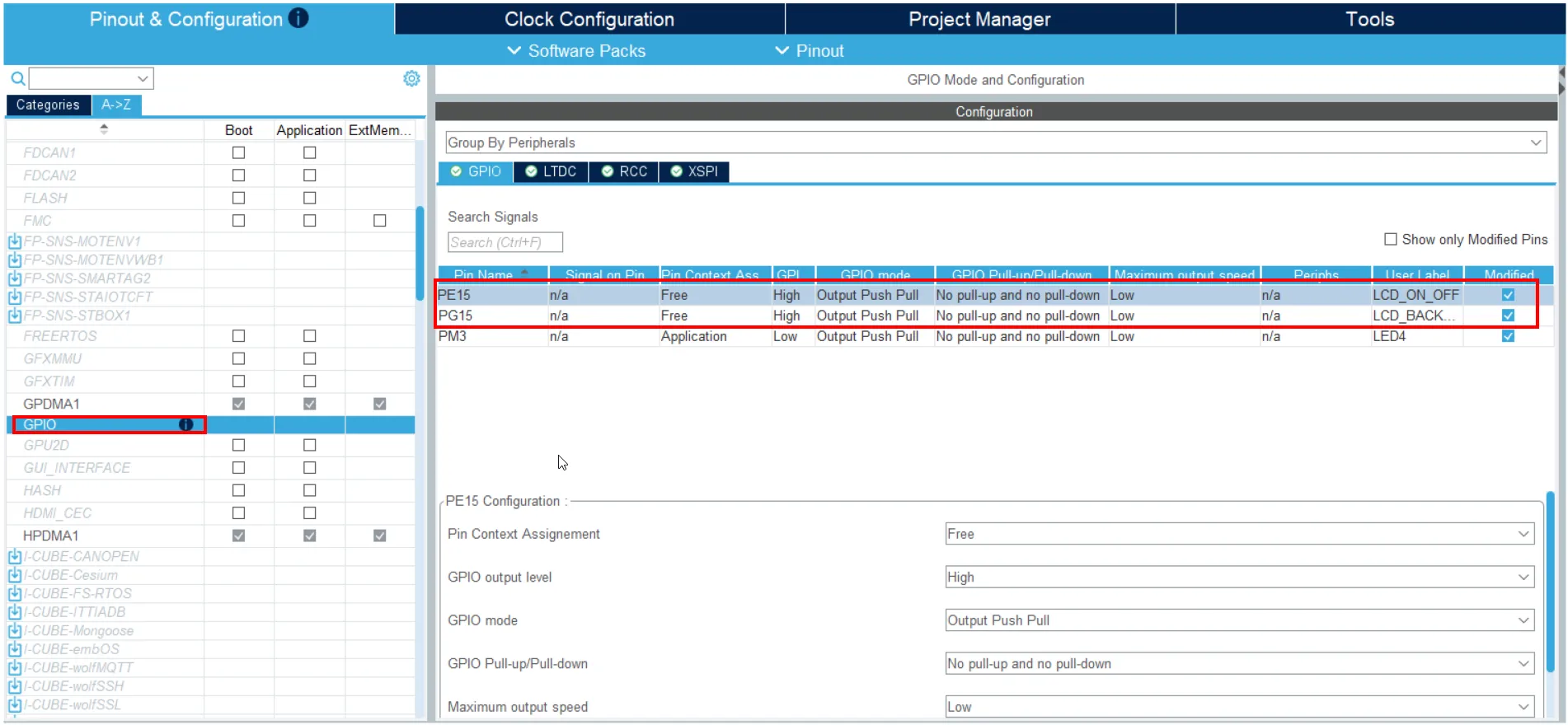
LTDC CONFIGURATION
Section titled “LTDC CONFIGURATION”The LTDC is enabled only in the Boot runtime context, because the bootloader is the one that configures it and shows the image. Its configuration is split into two tabs in STM32CubeMX: Parameter Settings (how to talk to the panel) and Layer Settings (what to show and where).
LTDC PARAMETER SETTINGS
Section titled “LTDC PARAMETER SETTINGS”These parameters describe the timing of the panel. The display on the board has a resolution of 800 x 480 pixels, and the LTDC needs to know, for each line and each frame, how long the synchronization pulse is and how many “invisible” pixels and lines there are before and after the visible area:
- Horizontal / Vertical Synchronization Width: duration of the HSYNC and VSYNC pulses.
- Back Porch (HBP / VBP): pixels (or lines) between the end of the sync pulse and the first visible pixel (or line).
- Active Width / Height: the visible area, 800 x 480 for this panel.
- Front Porch (HFP / VFP): pixels (or lines) after the last visible pixel (or line) and before the next sync pulse.
- Polarity: whether HSYNC, VSYNC, DE and the pixel clock are active high or active low.
These values come from the panel datasheet; if they are wrong, the image will be shifted, flicker, or not appear at all. Also remember that the LTDC needs its pixel clock, which is configured in the clock configuration (RCC) and must match the frequency that the panel expects.
================================================================================LTDC CONFIGURATION - STM32CubeMX (STM32H7S7L8HxH)================================================================================
[Device and Context]  - Microcontroller:                             STM32H7S7L8HxH  - Peripheral:                                  LTDC  - Runtime Contexts:                            Boot (Checked)
[Configuration > Parameter Settings]  > Synchronization for Width:    - Horizontal Synchronization Width:          8 pixels    - Horizontal Back Porch:                     7 pixels    - Active Width:                              800 pixels    - Horizontal Front Porch:                    6 pixels
  > Synchronization for Height:    - Vertical Synchronization Height:           4 lines    - Vertical Back Porch:                       2 lines    - Active Height:                             480 lines    - Vertical Front Porch:                      2 lines
  > Signal Polarity:    - Horizontal Synchronization Polarity:       Active Low    - Vertical Synchronization Polarity:         Active Low    - Not Data Enable Polarity:                  Active Low    - Pixel Clock Polarity:                      Normal input
  > Layer Default Color:    - Red:                                      0    - Green:                                    0    - Blue:                                     0================================================================================
LAYER SETTINGS
Section titled “LAYER SETTINGS”The LTDC supports up to two layers that can be blended on top of each other. For a splash image, one layer is enough. These are the main settings:
- Window Position: the area of the screen where the layer is drawn. Here it covers the full screen (0–800 horizontally, 0–480 vertically).
- Pixel Format: how each pixel is stored in memory. It must be the same format that the Python script uses to convert the image (You will see it in the next section), in this case RGB565 (16 bits per pixel: 5 bits red, 6 bits green, 5 bits blue). If the formats do not match, the image will still appear but with wrong colors.
- Blending: the alpha constant of 255 makes the layer fully opaque, and using “Alpha constant” for both blending factors means the layer is mixed only with that constant value, not with a per-pixel alpha (RGB565 has no alpha channel anyway).
- Layer Default Color: the color the layer uses outside its window or when it is disabled. With alpha 0 it is fully transparent, so it does not affect the result.
- Frame Buffer: the start address of the image in memory, which is the address of our
redBird_maparray, and its size in pixels: 401 pixels per line and 378 lines.
================================================================================LTDC CONFIGURATION - STM32CubeMX (STM32H7S7L8HxH)================================================================================
[Device and Context]  - Microcontroller:             STM32H7S7L8HxH  - Peripheral:                  LTDC  - Runtime Contexts:            Boot (Checked)
[Configuration > Layer Settings]  > Number of Layers:    - Number of Layers:                          1 layer
  > Windows Position:    - Layer 0 - Window Horizontal Start:         0    - Layer 0 - Window Horizontal Stop:          800    - Layer 0 - Window Vertical Start:           0    - Layer 0 - Window Vertical Stop:            480
  > Pixel Parameters:    - Layer 0 - Pixel Format:                    RGB565
  > Blending:    - Layer 0 - Alpha constant for blending:     255    - Layer 0 - Blending Factor1:                Alpha constant    - Layer 0 - Blending Factor2:                Alpha constant
  > Layer Default Color:    - Layer 0 - Alpha:                           0    - Layer 0 - Blue:                            255    - Layer 0 - Green:                           0    - Layer 0 - Red:                             255
> Frame Buffer: - Layer 0 - Color Frame Buffer Start Adress: (uint32_t)&redBird_map - Layer 0 - Color Frame Buffer Line Length: 401 - Layer 0 - Color Frame Buffer Lines: 378================================================================================Using python script to generate splash image
Section titled “Using python script to generate splash image”The LTDC cannot read a PNG file directly; it needs the raw pixel values in the selected pixel format. So we convert the image to an array of RGB565 values (one 16-bit value per pixel) and include it in the code as a C header file. I provided the Python script that I used to transform the example image.
Execute this command in the folder where the script is located to generate the .h file with all values of the converted image:
py pngToRGB565.py redBird.png redBird.hThe size of the result is easy to calculate: 401 x 378 pixels x 2 bytes per pixel = 303,156 bytes, about 296 KB. This is important for the next step.
Updating redBird.h file
Section titled “Updating redBird.h file”Once you have the new file created, we need to decide in which memory it will be stored. The STM32H7S7L8 has only 64 KB of internal flash, which is used by the bootloader itself, so a 296 KB image does not fit there. That is why we store it in the external flash of the board.
To do that, we put the array in a custom section called .xspi_flash, which we will create in the linker script in the next section.
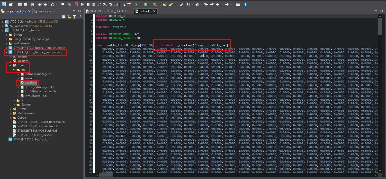
As you can see above, we move the new file into the file structure of the boot application and add the following compiler attribute to the array:
__attribute__((section(".xspi_flash")))This attribute tells the compiler to place the array in the .xspi_flash section instead of the default sections (.rodata or .data). Also declare the array as const: the image is read-only data, and this avoids the compiler or the startup code treating it as a variable that needs to be copied to RAM.
Updating linker file
Section titled “Updating linker file”In this part, we will update the linker script (STM32H7S7L8HXH_FLASH.ld). Why? During the build of a C or C++ program, the compiler generates the code and data, but it is the linker that decides the final address of each of them. The compiler attribute only gives the array a section name; the linker script is where we say that this section must be placed in the external flash. Without this change, the linker would not know where to put .xspi_flash.
First, we add the external flash to the MEMORY block. This tells the linker that there is a memory starting at 0x70000000 with a size of 128 MB, and that it is readable and executable (rx) but not writable from the program:
/* Memories definition */MEMORY{  RAM                    (xrw) : ORIGIN = __RAM_BEGIN,                               LENGTH = __RAM_SIZE  RAM_NONCACHEABLEBUFFER (xrw) : ORIGIN = __RAM_BEGIN + __RAM_SIZE,                  LENGTH = __RAM_NONCACHEABLEBUFFER_SIZE
  ITCM                   (xrw) : ORIGIN = 0x00000000,                                LENGTH = 0x00010000  DTCM                    (rw) : ORIGIN = 0x20000000,                                LENGTH = 0x00010000  SRAMAHB                (rw)  : ORIGIN = 0x30000000,                                LENGTH = 0x00008000  BKPSRAM                (rw)  : ORIGIN = 0x38800000,                                LENGTH = 0x00001000
  FLASH                  (xrw) : ORIGIN = __FLASH_BEGIN,                             LENGTH = __FLASH_SIZE  XSPI1_FLASH             (rx) : ORIGIN = 0x70000000,                                LENGTH = 128M}
Then, we create a new output section in the SECTIONS block. It collects every input section called .xspi_flash (or starting with that name) from all object files and places them in the XSPI1_FLASH memory. The ALIGN(4) lines keep the start and end of the section aligned to 4 bytes, which is a good practice for data that will be read by peripherals such as the LTDC:
/* ======================================================================== */ /* External Flash Section (Assets, Splashes, Raw Bitmaps) */ /* ======================================================================== */ .xspi_flash : { . = ALIGN(4); *(.xspi_flash) *(.xspi_flash*) . = ALIGN(4); } >XSPI1_FLASHLTDC Debug Settings
Section titled “LTDC Debug Settings”For this example, you need to add the external loader in the debug configuration. In the tutorial Initial Configuration of STM32H7S78-DK with STM32CubeMX: Bootloader Architecture and XIP Application, the boot project did not need it, but now it does.
Why? Because of redBird_map. The boot project now contains data at addresses in the external flash. The debugger can program the internal flash by itself, but it does not know how to write to the external flash memory. The external loader is a small program that the debugger loads into the MCU RAM to program that external memory. Without it, the image would never be written to the board.
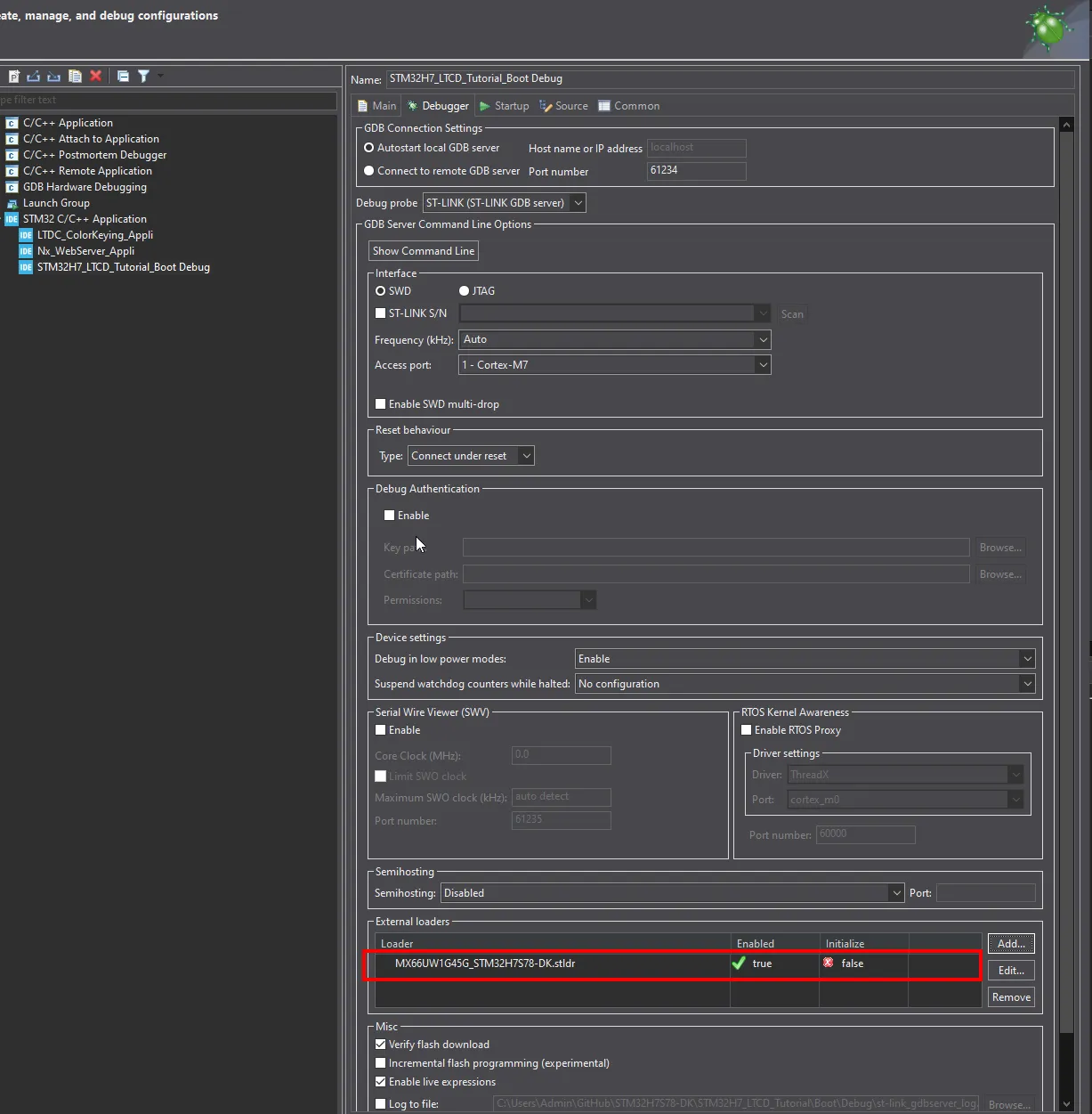
Checking splash image
Section titled “Checking splash image”During the debug session, you will notice that the image does not appear as soon as the LTDC is initialized. This is expected: the image lives in the external flash, and the LTDC can only read it after the bootloader has configured the XSPI interface in memory-mapped mode. Before that moment, the addresses at 0x70000000 are not accessible yet, so there is nothing valid to display.
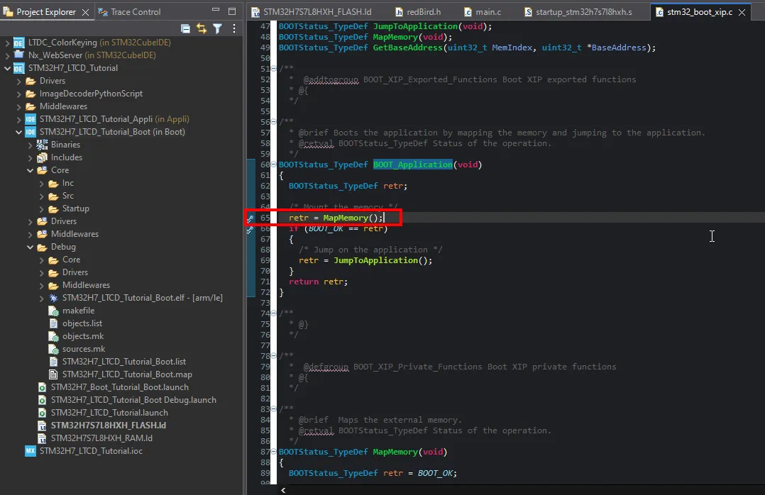
After the memory-mapped mode is enabled, press the continue button. When the debugger reaches the next breakpoint, just before jumping to the main application, the bird will appear on the screen!
Since the LTDC keeps reading the frame buffer by itself, the image will remain on the screen after the jump, as long as the application does not reconfigure the LTDC and keeps the external memory in memory-mapped mode.
Result
Section titled “Result”This is the final result of the tutorial. The bootloader configures the LTDC, enables the external flash in memory-mapped mode, and the splash image is displayed on the screen of the STM32H7S78-DK before jumping to the main application.
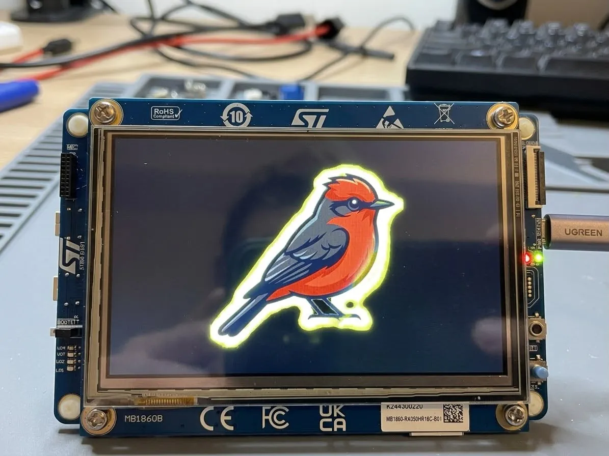
Example code
Section titled “Example code”The complete code for this example is available in the following repository:
- GitHub repository: STM32H7S78-DK
You can clone it with:
git clone https://github.com/rcocoletzim/STM32H7S78-DK.git